For the past few years, mobile devices have been continuously more powerful, yet more mobile. The last generation of high-end SoCs, specifically, NVIDIA's Tegra 3, Qualcomm's Snapdragon S4, and Samsung's Exynos 4 Quad, among others, have established a new standard for mobile performance by bringing quad-core CPUs into mobile devices, as well as taking mobile gaming to a whole new level, yet without sacrifying the power consumption of these SoCs, using solutions like the 4-PLUS-1 architecture inside the Tegra 3 (four performance cores, with one low power core to handle light workloads, draining much less power). After that evolution, these main competitors in the mobile SoC space needed decent successors that continued the trend of more performance with less power consumption, and the forthcoming generation doesn't dissapoint. The NVIDIA Tegra 4, Samsung's Exynos 5 Octa, and Qualcomm's Snapdragon 800 are each very impressive, each of which have one especially breathtaking feature.
All of these SoCs have one thing in common: their die process. Qualcomm has been using its 28nm process since last year, while NVIDIA is making a gigantic stride from its aged 40nm process to 28nm, while Samsung is upgrading the Exynos line from its own 32nm HKMG process to 28nm HKMG with the Exynos 5 Octa.
CPU
ARM's Cortex A15 CPU has already shown very impressive performance, only with two cores, in the Exynos 5 Dual SoC released (so far only) in the Nexus 10 tablet. With only two cores, the Cortex A15 topped almost all benchmarks, performing even better than every quad-core mobile CPU. In this generation of SoCs, we will be seeing double the already champion performance of the Exynos 5 Dual, since Cortex A15s in quad-core configurations will be common.
The NVIDIA Tegra 4 maintains the 4-PLUS-1 architecture used in the Tegra 3. The main, performance CPU cores will be four Cortex A15 core clocked at an impressive 1.9GHz, which is honestly more than a mobile device will ever need. Since so much performance would result in fast battery drain, NVIDIA included a fifth Cortex A15 core, but this one is designed for low power, in other words, to handle light workloads such as playing video and music, for example, and power gating the four power hungry Cortex A15 cores, hence dramatically increasing power efficiency. The fifth A15 core can run at up to 825MHz, which is roughly the performance of a single 1.6GHz Cortex A9 core. The Tegra 4's little brother, the mid-range Tegra 4i, will have a slightly different CPU. While still employing 4-PLUS-1, the 4i will not use A15 cores, but a newer, improved version of the old Cortex A9; the four A9 cores will be able to run at up to 2.3GHz, which should bring the old CPU's performance up to scratch. A fifth companion core will also be used with the Tegra 4i.
Samsung's Exynos 5 Octa even has a name that calls people's attention to the CPU, since the name implies the first SoC to integrate 8 CPU cores. But that doesn't mean that we'll see 8-core performance on a mobile device. The Octa is actually the first SoC to use ARM's big.LITTLE setup. A similar concept to NVIDIA's 4-PLUS-1, the Octa makes use of four Cortex A15 cores with a maximum clock speed of 1.8GHz, for heavy workloads, and a much smaller quad-core Cortex A7 cluster, running at up to 1.2GHz, to handle the lighter of workloads. A Cortex A7 CPU is similarly performing to a Cortex A9, only with better power efficiency. So the low power cores can actually deliver pretty high performance at much less power consumption, than roughly a quad-core Cortex A9 @ 1.2GHz (Tegra 3 T30L, for example). It is fair to assume that the low-power Cortex A7s will be in usage much more often than the companion core in the Tegra 4, which might give Samsung the advantage in terms of power consumption.
Qualcomm is known for not licensing complete ARM CPUs, but instead they license the architecture and modify it to make a custom CPU, which they've been calling Krait since the Snapdragon S4. Krait CPUs tend to fare pretty well in terms of power consumption as well. For the still quite distant Snapdragon 800, Qualcomm will employ a new custom CPU, the Krait 400. The Snapdragon 800 will employ four Krait 400 cores, which will be able to run at a stunning max frequency of 2.3GHz. Krait cores have a special characteristic about them, that they can have different cores running at different clock speeds, based on the workload, which can yield some good results in terms of energy efficiency.
The GPU + Memory
Gaming has become a very important aspect in mobile technology. As such, SoC manufacturers, especially Apple, invest a lot in integrating excellent GPUs in their SoCs, and the newest offerings from Samsung, NVIDIA and Qualcomm are no different. NVIDIA, ironically, has never really had industry leading mobile GPUs in its Tegra series, but the same can't be said about the GPU in the Tegra 4. Designed by NVIDIA, of course, the new ULP GeForce is an enormous improvement over the last generation, as the Tegra 4 has a total of 72 graphics "cores", up from 12 in the Tegra 3. Only that is already a 6x improvement. However, Tegra 4 remains the only modern SoC whose GPU uses discrete pixel and vertex shaders, as opposed to a unified architecture. The 72 cores in the Tegra 4 are divided into four pixel units, each of which contain 12 ALUs (that's what NVIDIA refers to as a "core"), as well as six vertex units, each containing 4 ALUs. The max clock speed for the GPU is an impressive 672MHz. At this clock rate, the Tegra 4 has 96.8 GFLOPS processing power; an indrustry leading result, finally. In fact, recent benchmarks show the Tegra 4 to slightly outperform the mighty iPad 4 for the first time. The Tegra 4i uses the same GPU architecture as the Tegra 4, but is watered down, with 60 total cores. The 4i has the same 48 pixel shader ALUs as the Tegra 4, although instead of spreading these 48 ALUs over four pixel units, the Tegra 4i has two larger pixels units, each containing 24 pixel ALUs, while the amount of vertex ALUs gets cut by half in the 4i, with only three vertex units with 4 vertex ALUs each. At a slightly lower clock rate of 660MHz, the Tegra 4i's GPU has a max theoretical performance of 79 GFLOPS, which is still very impressive. While the GPUs' performance is impressive, it's features aren't as impressive, as Tegra 4 is one of the few modern GPUs that don't offer full OpenGL ES 3.0 compatibility (a few features are available, however).
Given that we're now on a time where resolution is being a big priority for mobile devices, these next-gen SoCs just had to offer brutal memory bandwidth. This has always been a concern in the Tegra SoCs, but NVIDIA has finally decided to eliminate that issue. The Tegra 4 chip, destined at high-end tablets, which by now are expected to have a resolution of at least 1920 x 1200, will probably handle high resolutions easily, since it's memory interface is an impressive, yet not innovating dual-channel DDR3L-1866. This should in theory deliver enough fill rate for playing even the most complex games on a very high resolution tablet (2560 x 1600), especially considering NVIDIA's claims that the GPU is optimized for using memory bandwidth more efficiently. As the Tegra 4i is destined to be inside smartphones, it will generally have to handle lower resolutions, so NVIDIA opted for a less powerful, less power hungry memory interface, perhaps a bit too much though, as the Tegra 4i has only a single-channel LPDDR3 memory. In a Package-on-package (PoP) configuration, where the memory is soldered onto the SoC, the Tegra 4i will support up to LPDDR3-1600, which is just as much as the last-gen Tegra 3. If the memory is embedded with the SoC (discrete), however, the 4i will support up to single-channel LPDDR3-1866, half of what the Tegra 4 can do, which isn't really enough, especially considering 2013 will be 1080p smartphone year.
The Exynos 5 Octa represents a big departure from its usual GPU tradition. The Exynos line has always used ARM's Mali GPUs, but the Exynos 5 moves to a PowerVR GPU, in this case, the PowerVR SGX544MP3, practically identical to the GPU used in the iPad 3. ImgTech's GPU line has a very mature unified shader architecture, and it doesn't at all support OpenGL ES 3.0. There are 12 unified shader units in this GPU (four per module, as this is the MP3, hence, three modules), each of which contain four ALUs. But the difference between the iPad 3's SoC and the Exynos Octa is that the Octa's SGX544MP3 is clocked much higher, at 533MHz. That equates to 51.1 GFLOPS peak performance, which is almost exactly in between the iPad 3's 32 GFLOPs and the iPad 4's 71.6 GFLOPS. Looking at these figures, it seems that the Exynos 5 Octa won't be keeping up with the competition at all. Its performance, at least in paper, pales compared to NVIDIA's competitive offering. The memory interface of the Octa isn't yet known, but it will probably be somewhat alike, if not better than, its little brother, the Exynos 5 Dual, which has a dual-channel DDR3-1600 memory interface, which should actually be good even for 2560x1600 tablets.
Unfortunately, Qualcomm never discloses any information about its Adreno GPUs, so all we know is that the Snapdragon 800 will debut the Adreno 330 GPU, which should provide the same feature set as the current Adreno 320, but with higher performance capabilities. Considering that currently the Adreno 320 is already one of the most powerful GPUs available, a lot is expected from the 330. Aside from performance, the 330 will be an OpenGL ES 3.0 capable graphics processor, and that's pretty much all that is known. But the bottom line is, when the Snapdragon 800 debuts, it will probably boast the best mobile GPU, with the likes of even surpassing the Tegra 4's beefy GPU. Much like the Exynos 5 Dual, and probably the Octa too, the Snapdragon 800's memory interface will be of two DDR3-1600 channels.
Conclusion
All of these SoCs have many similarities, well, except for the Tegra 4i, which is clearly destined to be a mid-range SoC, and cannot compete with any of the other top-end SoCs. These are similar in the way that they all use 28nm process, they're all quad-cores of brand new CPU architectures, and all of them have some method of increasing power consumption. In the case of NVIDIA and Samsung, the solution is to increase power efficiency by adding in low power cores to handle simple workloads, while Qualcomm does chooses to have their cores with asynchronous clock rates. Their key difference comes in terms of their GPUs. While Samsung, oddly, chooses to use a GPU that isn't very competitive, NVIDIA and Qualcomm are taking gaming performance very seriously and improving their GPU offerings. In terms of memory, in fact, all of these SoCs have nearly identical memory interfaces, so the key difference will be how efficiently the CPU and GPU use the memory bandwidth. But ultimately it all comes down to when these SoCs are being released. Technically, the Exynos 5 Octa already debuted in the GT-I9500 variant of the Galaxy S4, but most S4s are the I9505 variants with a Snapdragon 600 SoC, so there are few devices shipping with the Octa due to low availability of the SoC. The Tegra 4 is supposed to break cover in May/June with the NVIDIA SHIELD gaming portable, and the Snapdragon 800, as well as the Tegra 4i, are supposed to debut later this year.

Mostrando postagens com marcador system on chip. Mostrar todas as postagens
Mostrando postagens com marcador system on chip. Mostrar todas as postagens
domingo, 19 de maio de 2013

sexta-feira, 16 de novembro de 2012
Nexus 10's SoC, Samsung Exynos 5250 review
Google's new Nexus 10 tablet, which was developed alongside Samsung, features some killer specs, most notably, the unsurpassed screen resolution of 2560 x 1600 pixels. This immense resolution results in a fine 299ppi pixel density, surpassing even the iPad's 264ppi display. However, performance demand is proportional to resolution, therefore, to be able to power such a powerful display, Google needed an extremely powerful SoC, something of the likes of Apple's A5X SoC. Well, Google has done right in choosing Samsung's brand new Exynos 5250 SoC. The Exynos 5250 is built on Samsung's successful 32nm HKMG (High-K Metal Gate) process.
The CPU
Less than a year ago, all SoC manufacturers were bound to Cortex-A9 CPUs, so there was no real competition in terms of single-threaded performance, since it was all the same. Today, of course, the story is different. ARM's Cortex-A15 architecture leveraged certain ARM-based CPU designing companies into making similar architectures. Currently, we have three new architectures competing with each other, Qualcomm's Krait, Apple's Swift, and ARM's Cortex-A15. The real difference between these is single-threaded performance. While the Swift didn't really surprise anyone, and Krait, well, did a pretty good job, the Cortex-A15 is just astounding on a per-core basis. Indeed, one A15 core is about twice as fast as one Krait core. Now, The Exynos 5250 has two A15 cores clocked at 1.7GHz, which theoretically should translate into the best mobile CPU performance ever seen.

The Exynos 5250 in the Nexus 10 distinguishes itself clearly from the rest of the competition, and it does that, while also being one of the few who have only two cores (granted, it has the highest clock). Comparing it to the only other dual-core processor there, the Swift, found in the Apple A6X flagship SoC, we can see that per-core efficiency is unprecedented in the Cortex-A15.
Memory interface
The main constraint that a high-resolution screen poses is memory bandwidth. Considering how bad Android devices' SoCs usually do in terms of memory bandwidth, the Exynos 5250 was a true surprise. This SoC contains a dual-channel DDR3-1600 (800MHz) memory controller, bringing the theoretical memory bandwidth to a PC-class 12.8GB/s. Apple's A5X and A6X chips (both powering an iPad's Retina display) both achieve the same bandwidth as the Exynos 5250, theoretically speaking, only with a much wider memory interface (quad-channel LPDDR2-1066). That said, the Exynos 5250 is the first non-Apple SoC ever to be able to power such a fine display as the Nexus 10's.
The GPU
Another big surprise that comes with the Exynos 5250 is the brand new Mali-T604 GPU, built by ARM. It is the first GPU to use ARM's new midgard architecture, which is a new unified shader architecture. As we will see in the benchmarks below, the Mali-T604 kills the GPU inside the A5X, but lags behind the A6X. At any rate, it is by far the best GPU on the Android space.

Despite the theoretical memory bandwidth of the Exynos 5250 being equal to Apple's A6X, we clearly see that there is a huge gap between the A6X's maximum fill rate and the Exynos' maximum fill rate. Aside from the A6X, the Exynos 5250 shows excellent fill rate, leaving the other competition in the dust, and it should surely be able to handle properly the Nexus 10's immense display resolution.


Unfortunately, we see in the Offscreen Egypt HD test that the iPad 4's PowerVR SGX554MP4 GPU is actually significantly stronger than the Mali-T604, which only edges ahead of the Adreno 320. Still, it performs very well, and is the most powerful GPU on the Android space. The Onscreen test shows us the sad reality that the 2560 x 1600 display is a bit too demanding for the Mali-T604. The overall weaker GPU, combined with the significantly higher reolution, resulted in the Nexus 10 performing much worse than the iPad 4. Despite that, and taking into consideration the unprecedented resolution, the Mali-T604 does offer some reasonably good performance, and should suffice for most gaming uses.


Here is the part where Mali GPUs always get disappointing. ARM's GPUs have never been very good at their triangle throughput. We can see that the T604's midgard architecture has really improved Mali's triangle throughput, looking at the improvement since the last-gen Mali-400MP, but it is still humiliating for ARM. The triangle throughput isn't even comparable to what the iPad 4 offers, and even the 1-year-old NVIDIA Tegra 3 edges ahead (granted, triangle throughput is NVIDIA's forte). It should be good enough to power most games, but in situations where the polygon count is very high, the weak triangle throughput could act as a performance bottleneck.
Conclusion
We've seen that the Samsung Exynos 5250 has its strong points, but we've also seen a weak side to Samsung's new flagship SoC, although the vast majority of the SoC's features are excellent. The Exynos 5250 is a very interesting SoC because it uses new architectures for almost everything; it is the first to use ARM's Cortex-A15 CPU design, and also the first to have ARM's new Mali-T604 GPU. As a result, the midgard architecture also debuts with the Exynos 5250. Unlike most of the current SoCs, the Exynos 5250's features are all fine, from the die process to the CPU, the GPU and the memory controller. We also get the best from power efficiency, thanks to Samsung's 32nm HKMG process and the Cortex-A15, which proved to be quite an efficient CPU. The Nexus 10 is a very demanding device, and the Exynos 5250 is the only SoC capable of satisfying the new slate's needy demands.
sexta-feira, 2 de novembro de 2012
Apple A6X SoC Analyzed: Dual-core Swift and quad-core PowerVR SGX 554MP4

So we have the iPad 4 coming out today, and Apple previously made a claim that the SoC (System-on-Chip) powering it would be twice as fast as the previous generation iPad's A5X SoC. Well, we just got some benchmark results on the iPad 4, and they only seem to prove that indeed, the A6X is at least twice as good as the A5X, and in some benchmarks even more than twice.
CPU first, of course. The A6X features a dual-core CPU based on a custom architecture made by Apple, named Swift, much like in the iPhone 5, except the A6X's CPU is clocked at 1.4GHz, as opposed to 1.3GHz in the A6. The performance of the A6X CPU is ok, and is able to keep up with what the Android competition currently offers, not more, not less.
 CPU performance has never been Apple's focus, but in the iPad 4 it's ok, at most. At the very least, it matches (and slightly outperforms) the Galaxy S III, at the same clock speed but with two cores less, but it is still destroyed by Samsung's Exynos 5 Dual, Qualcomm's Snapdragon S4 quad-core, and to some extent NVIDIA's Tegra 3. On a per-core performance perspective, Apple's Swift is very good, although the per-core king of the hill now is the new Exynos 5250.
Before going into the GPU, I'll quickly talk about the memory interface in the A6X. Like in the A5X, the memory interface in the A6X is the widest one ever seen on a mobile device. The A6X features a quad-channel LPDDR2-1066 memory controller, bringing the theoretical memory bandwidth up to an impressive 12.8 GB/s. This is, of course, necessary to power the 2048 x 1536 display in the iPad 4.
And then there's the GPU, the biggest change in the A6X. Apple has always been known for pushing the mobile graphics performance forward, and it has done just that again. The A6X features a stunning PowerVR SGX554MP4 quad-core GPU. The main difference between the 543 used in previous-gen iPads and the 554 is a doubling in ALU count per core. having four cores, this, therefore, means that the 554MP4 has a total of 32 ALUs, as opposed to 16 ALUs in the 543MP4, therefore, at the same clock speed, we get doubled performance since the A5X. If we assume that the clock speed remains unchanged, this results in a revolutionary 64 GFLOPS of peak theoretical performance. Apart from that, we get the same PowerVR goodness Apple has always benefited from; a TBDR (Tile Based Deffered Renderer) with unified shader architecture.


The Offscreen Egypt HD test shows us that the SGX 554MP4 is much more powerful than the Adreno 320, but in the Onscreen test, what puts the iPad 4 behind the Adreno 320-boasting PadFone 2 is the iPad 4's immense resolution.

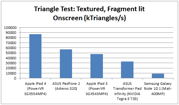
As we can see, the iPad 4 is at the top in every benchmark, except for the Egypt HD Onscreen test, where the iPad's large resolution limits its performance, but at any rate, the margin between the PadFone 2 and the iPad 4 in the onscreen test is almost insignificant. We can see that, once again, Apple has managed to put itself at the very top of mobile graphics performance, by a very large margin.
All of that power results in a giant die area of 123mm2. It is really very large, considering that it is build with Samsung's 32nm HKMG (High-K Metal Gate) process. The A6X sets a new benchmark for other competitors to reach. Samsung's Exynos 5250, despite being from the same generation as the A6X, has already lost to it. The warning goes to NVIDIA, mainly. The graphics company's upcoming Tegra 4 'Wayne' SoC is rumored to have a quad-core Cortex-A15 CPU (which is double the performance of the already champion Exynos 5250), and a Kepler based GPU that allegedly has 24 cores, and will be built on 28nm process. We can rest assured that a quad-core Cortex-A15 will be more than enough, and 28nm will also bring the Tegra series up to date. A Kepler GPU seems promising, too, but NVIDIA will have to work hard if it wants to beat the new graphics performance (and also memory bandwidth) king of the hill, the Apple A6X.
Assinar:
Postagens (Atom)